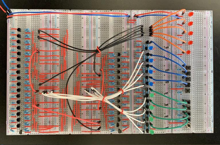
Building a 4-bit adder from transistors
Overview
During lockdown,
- 48 transistors
- 154 resistors
- 13 LEDs
- 10 switches
- 7m wire
- 5 breadboards

The addition circuit
The rules of binary and decimal arithmetic are quite similar, with the primary difference being the base of the number system used. When adding two binary numbers, one starts by adding the rightmost column of bits and works towards the left. Bit sums greater than 1 are carried over to the next column. This process, known as “carry propagation,” results in two outputs: the sum and the carry bit. The carry bit is subsequently used as a third summand in the addition of the next pair of digits. The table below shows how to add two bits
| A | B | Carry-in | Sum | Carry-out |
|---|---|---|---|---|
| 0 | 0 | 0 | 0 | 0 |
| 0 | 0 | 1 | 1 | 0 |
| 0 | 1 | 0 | 1 | 0 |
| 0 | 1 | 1 | 0 | 1 |
| 1 | 0 | 0 | 1 | 0 |
| 1 | 0 | 1 | 0 | 1 |
| 1 | 1 | 0 | 0 | 1 |
| 1 | 1 | 1 | 1 | 1 |
The logic circuit used to add A, B, and the carry-in bit is known as a full adder, which is more complex than the simpler half-adder used for adding the rightmost bit column that does not have a carry-in bit. The standard logic circuit for half adders consists of only an AND and XOR gate, however, these circuits require a lot of electrical components.
Here is a table with some bit operations on A and B for reference.
| A | B | AND | NAND | OR | NOR | XOR | ||
|---|---|---|---|---|---|---|---|---|
| 0 | 0 | 0 | 1 | 0 | 1 | 0 | ||
| 0 | 1 | 0 | 1 | 1 | 0 | 1 | ||
| 1 | 0 | 0 | 1 | 1 | 0 | 1 | ||
| 1 | 1 | 1 | 0 | 1 | 0 | 0 |
A key consideration in designing my calculator was the construction of the addition circuit using logic gates while minimizing the number of electrical components needed. I eventually found that building the half and full adders entirely out of NOR gates minimizes the number of electrical components needed as each NOR gate requires only one transistor and three resistors. This approach allowed me to build half and full adders using only 5 and 9 transistors, respectively. An added benefit of this approach was that using only one type of logic gate kept the final circuit more organized.
To create a 4-bit adder, multiple adders are chained together by connecting their carry-out terminal to the next adder’s carry-in terminal as shown in the figure above. The first adder in the chain does not have a carry-in and, thus, the simpler half-adder is used. The carry-out bit of the last adder in the chain is considered to be part of the sum.
NOR gates from transistors
The “Engineer’s Mini-notebook: Digital Logic Circuits” (Radio Shack, 1985) on page 6 shows how to build simple logic gates using resistor–transistor logic (RTL). The middle circuit in the figure above shows their version of a NOR gate which was constructed from 2 NPN transistors and 3 resistors. I used a simplified version of the NOR gate which only used one transistor (see the right circuit above).
Connecting both inputs to a single transistor base does not impact the circuit in most cases. However, when a voltage is applied to both inputs A and B, the base current will be twice as high as that of the 2-transistor NOR gate. This wasn’t much of an issue though since my PN2222A transistors can handle higher currents than my power source could produce. Additionally, the transistor’s specifications indicate that its collector current is nearly invariant to changes in the base current once the transistor is saturated.
For more complex logic circuits, it may be appropriate to calculate the optimal resistance values using specialized software that takes into account fan-out, optimal operating voltages, etc.
The memory circuit
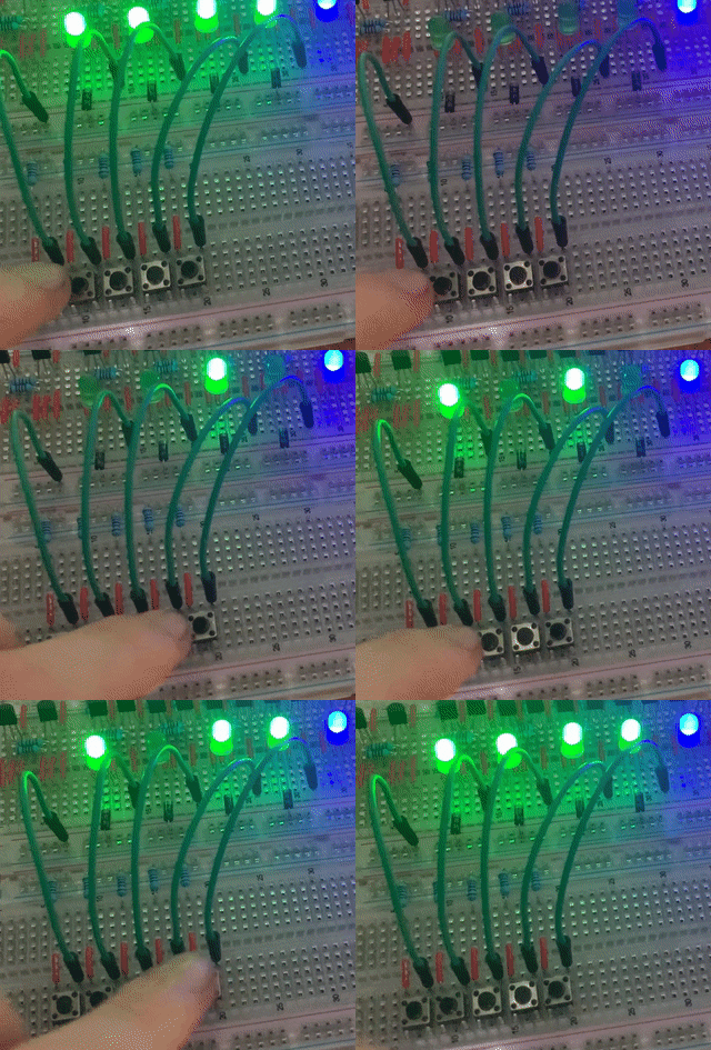
To store my calculator’s input numbers, I used a simple flip-flop whose logic circuit you can see above. Just like the half and full adders, I built the flip-flop entirely from NOR gates. According to Wikipedia, “Static RAM (SRAM) consists of flip-flops, a bistable circuit composed of four to six transistors.” However, since I used a simplified version of the standard NOR gate, I was able to build mine out of only 2 transistors. As the GIF below demonstrates, the memory worked as expected.

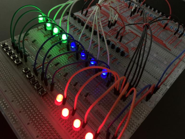
The completed calculator


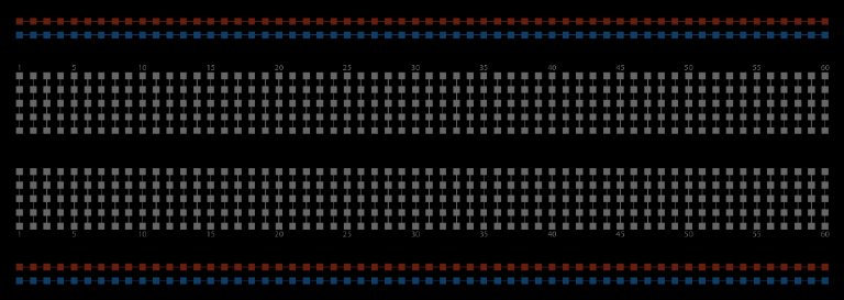
Breadboard design template

I made this breadboard design template to sketch out some designs and optimize the layout of my circuits prior to building them. It can be imported into GoodNotes or printed out -I made a light version of it too. The breadboard template can be downloaded using this link.

